The way of calculating jitter of a clock signal from the phase noise measured with the signal analyzer is mentioned.
Application
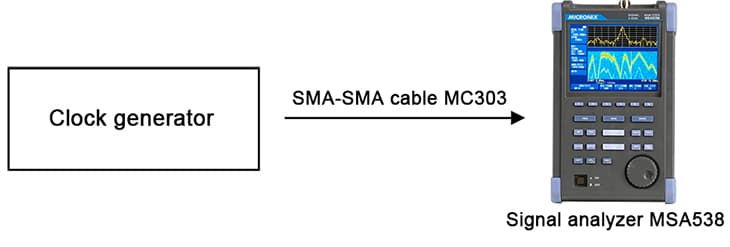
Connection block diagram
Solution
- The clock jitter is computable from the phase noise level measured with the signal analyzer.
- The instantaneous jitter can also measured by real time acquisition.
Moreover, it is also possible to obtain the RMS jitter for a long period of time by averaging.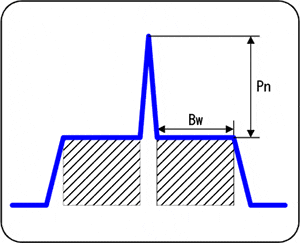
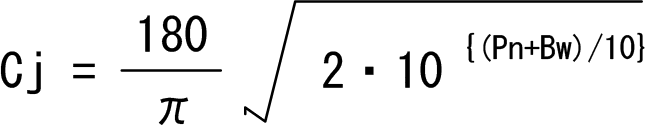
The spectrum shown at left is obtained when a clock signal with PLL is measured by the signal analyzer. In this case, the noise component which causes a clock jitter can be approximated by the area of shaded region. The clock jitter Cj (Deg) is obtained from the following equation based on the phase noise Pn (dBc/Hz) and the bandwidth Bw (Hz).
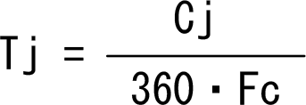
When the clock frequency is Fc [Hz] , the jitter time Tj [s] is as follows.
- In case of Fc=1GHz, the values of Cj and Tj based on typical phase noise and bandwidth are shown in table below.
- Cj[deg]
Phase noise
[dBc/Hz]10kHz
BW100kHz
BW1MHz
BW1MHz
BW-60 8.10 25.62 81.02 256.23 -70 2.56 8.10 25.62 81.02 -80 0.81 2.56 8.10 25.62 -90 0.26 0.81 2.56 8.10 -100 0.08 0.26 0.81 2.56 - Tj[ps]@1GHz
Phase noise
[dBc/Hz]10kHz
BW100kHz
BW1MHz
BW1MHz
BW-60 22.51 71.18 225.06 711.75 -70 7.12 22.51 71.18 225.06 -80 2.25 7.12 22.51 71.18 -90 0.71 2.25 7.12 22.51 -100 0.23 0.71 2.25 7.12
System configuration
| Signal analyzerMSA538 | x 1 |
| Lithium-ion battery [MB400] | x 1 |
| SMA-SMA cables1.5m [MC303] | x 1 |
| Adapter N(P)/SMA(J) [MA306] | x 1 |
Products introduction
[products skus="msa538,mb400" orderby="date" order="asc" columns="3"]
Please feel free to contact us.
If you want to verify 5G, customize a radio wave shield box, or need product repair, please do not hesitate to contact us about any small matter.