Any phase-modulated signal can be output.
Overview
Currently, the wireless communication is widely used even in consumer electronics products as well as in mobile
phone and digital terrestrial TV. As the handling amount of data is increasing, the modulation method has
been also improved. The phase modulation is a mainstream now.
How a phase-modulated signal is output from MSG703 will be described in this paper.
What's a vector signal generator ?
The standard signal generator generates only a sine wave signal but the vector signal generator modulates a
sine wave signal by the phase based on IQ data (I: in-phase component, Q: quadrature-phase component).
In other words, it means the following equation.
Vector=IQ modulation
Basic knowledge of phase modulation
In modulation system, there are AM and FM of analog method and ASK (Amplitude Shift Keying) and FSK (Frequency Shift Keying) of digital method. There is also PSK (Phase Shift Keying) of digital method as well.
Among these, PSK is the most popular recently. There are BPSK, QPSK, π / 4QPSK and so on in PSK system.
In addition, there is QAM including the information of amplitude.
The radio waves propagating in the air can be considered as single communication channel if the carrier frequency is single. However, some bits can be put on this single communication channel in PSK system.
In other words, it can be considered that some communication channels exist.
The number of bits is one bit in BPSK, 2 bits in QPSK and 6 bits in 64QAM. The increase of the number of bits means that the transmission amount per unit time increases. 64QAM will be six times transmission amount of BPSK.
Glossary
- PSK:Phase Shift Keying
- BPSK:Binary Phase Shift Keying, 2-level
- QPSK:Quadrature Phase Shift Keying, 4-level
- π/4QPSK:The orthogonal coordinate axes are rotated by 45 degrees each symbol, 4-level
- QAM:Quadrature Amplitude Modulation
- 64QAM:The information can be sent by 64-level.
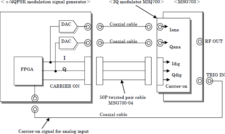
Explanation of IQ modulator MIQ700
The IQ modulator MIQ700 which is an option of MSG703 series is explained below.
Block diagram
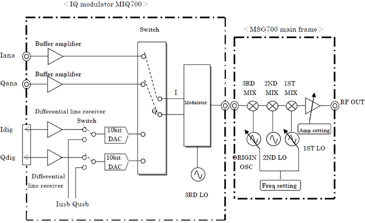
$$ \begin{cases} Iana、Qana:Analog IQ signal \\ Idig、Qdig :Digital IQ signal \\ Iusb、Qusb :USB data IQ signal \\ 1ST,2ND,3RD LO:1ST,2ND,3RD local oscillator \\ \end{cases} $$
Input conditions
- Analog input
Full scale voltege:IQ each ±600mV
Input impedance:50Ω
Baseband bandwidth :10MHz max(RF bandwidth 20MHz max) - Digital input
IQ bit number:each 10 bit
IQ data format:2’s complement
Rate:80MSPS max(bandwidth 10MHz max)
- USB data input
It's modulated by the data written in the USB memory
Generation ofπ/4QPSK modulation signal
This section describes how to generate π/4QPSK modulation signal used in ETC2.0. Regarding the regulation, refer to ARIB STD-T75.
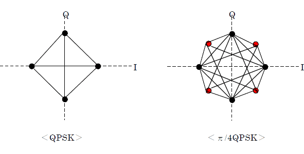
[0,π/2, π, π/2]plane is used in QPSK, but the whole of plane shifts "π/4" each symbol in π/4 QPSK.
In other words, if [0, π/2, π, -π/2] plane is used at a certain symbol, [π/4,3π/4, -3π/ 4, -π/ 4] plane is used at the next symbol. The amount of both informations of QPSK and π/4QPSK is 2 bit (four levels), but the output amplifier will be easy to design because the transition region of data in π/4 QPSK does not pass through zero volt as shown in the constellation figure below.
Generation of input signal to IQ modulator
First, the IQ signal, which is supplied to IQ modulator MIQ700, should be generated.
This time, how to generate IQ signal will be described based on ARIB STD-T75 (DSRC standard) which is used
in ETC2.0.
The circuit of block diagram described in next section can be easily realized by using FPGA (field programmable
gate array). Analog input [Iana, Qana] or digital input [Idig, Qdig] is input to IQ modulator MIQ700.
Then, π/4QPSK signal can be output from RF OUT connector of MSG703.
Block diagram
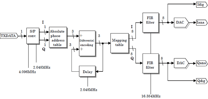
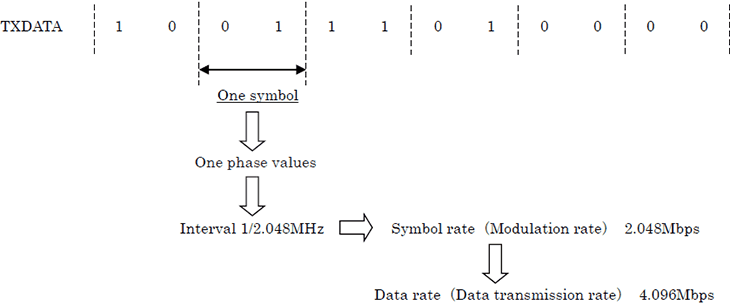
- TXDATA
Serial raw data. 4.096Mbps. - S/P conversion
Serial / parallel conversion. Serial raw data 2 bits (I and Q) is equivalent to one symbol. - Absolute phase address table
The phase Δ Φ makes correspond to 3 bits of absolute phase address so that the calculation of differential encoding may be easy. - Differential encoding
The current phase is added to the previous phase. The differential encoding regulation is defined as shown in the table below in ARIB STD-T75.I Q ΔΦ Absolute phase address 0 0 π/4 001 0 1 3π/4 011 1 0 -π/4 111 1 1 -3π/4 101 - Mapping table
The phase data are assigned on the coordinate values of I and Q.Phase data Phase I Q 000 0π 1 7F 0 00 001 π/4 1/√2 5A 1/√2 5A 010 π/2 0 00 1 7F 011 3π/4 -1/√2 A6 1/√2 5A 100 π -1 80 0 00 101 -3π/4 -1/√2 A6 -1/√2 A6 110 -π/2 0 00 -1 80 111 -π/4 1/√2 5A -1/√2 A6 8-bit / 2's complement
- FIR filter
The baseband band-limited is required so that the spectrum doesn't spread to adjacent channels.
$$ \begin{eqnarray}H(f) \begin{cases} 1@ 0 \leqq|f| \lt(1-α)/2T \\ \cos^{2}[(T/4α)(2π|f|-π(1-α)/T)]@(1-α)/2T\leqq|f|\lt(1+α)/2T \\ 0@(1+α)/2T\leqq|f| \\ \end{cases} \end{eqnarray} $$ $$ \begin{cases} ・T=1/2048(ms)(1/T=2.048 MHz)\\ ・Roll off rate α=1.0 \\ ・The phase characteristic of H (f) must be linear. \end{cases} $$
ARIB STD-T75 prescribes to use the following formula of Nyquist characteristic H (f).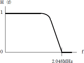
Explanation of differential encoding
The differential encoding will be concretely described using actual numbers.
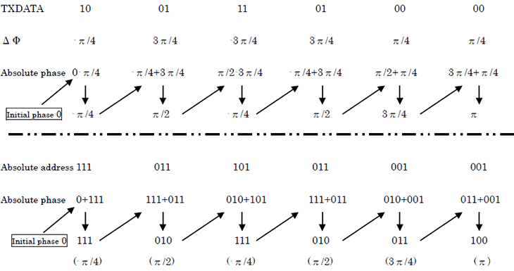
- It's shown that [0, π/2, π, -π/2] plane and [π/4,3π/4, -3π/4, -π/4] plane are alternately appeared every symbol.
- It's shown that the absolute phase is the same even if calculated by the absolute address.
Transmission rate
Generation of π/4QPSK
Connection block diagram
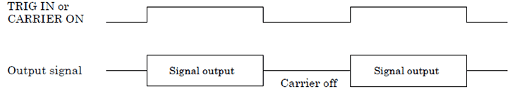
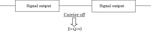
Burst control
In general, on communication system, data is divided into slot and then sent. The period between slot and slot
will be the carrier-off state. In short, it will be a burst signal. In general, the period of carrier-off will be in
receiving state.
MSG703 can perform the burst control for analog input and digital input.
In case of analog input, "Carrier on signal" is input from "TRIG IN" connector on the front panel. In case of
digital input, one pin in the digital input connector (but, differential input) is assigned to "CARRIER ON".
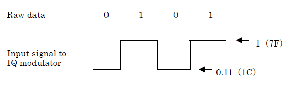
Possible of outputting ASK modulating signal
Using the IQ modulator MIG700, the ASK (Amplitude Shift Keying) signal can be also output.
I:Magnitude of amplitude Q:Always zero
On the other hand, the modulation depth is calculated by the following equation.
Modulation depth=(Vmax-Vmin)/(Vmax+Vmin)
For example, in case of the modulation depth = 80% and Vmax = 1 (7F) ;
Then, Vmin=0.11(1C)
The number in parentheses is expressed in 8-bit data.
Easy method for modulation signal generation
Without using hardware as described in "Generation of π/4 QPSK modulation signal", the method of generating
easily modulation signal is described below. It'll be achieved by calculating the generating method described in
this item on PC (personal computer). The modulation data created on PC is stored in USB memory, and then this
USB memory is inserted into "USB A plug" on the front panel of MSG703.
"IQ input signal" of MSG703 is set to "LIST data".
If the career-off state is necessary, IQ data in USB memory should be set to I = Q = 0.
※Data capacity:each IQ 10-bit × 8,192 words maximum
Readout rate:100Hz to 40MHz、100Hz step
Products introduction
[product sku="msg703"]
Please feel free to contact us.
If you want to verify 5G, customize a radio wave shield box, or need product repair, please do not hesitate to contact us about any small matter.